Purpose
The RT9055 is a dual channel, low noise, and low drop Regulator sourcing up to 300mA at each channel. Its input voltage range is from 1.5V to 5.5V and provides an adjustable regulated output voltage from 0.9V to 3.5V while delivering up to 0.3A of output current. This document explains the function and use of the RT9055 evaluation board (EVB), and provides information to enable operation, modification of the evaluation board and circuit to suit individual requirements.
Introduction
General Product Information
The RT9055 is a dual channel, low noise, and low drop Regulator sourcing up to 300mA at each channel. The input voltage range is from 1.5V to 5.5V.
The RT9055 offers 2% accuracy, extremely low dropout voltage and extremely low quiescent current (only 29µA per LDO). The shutdown current is near zero which is suitable for battery powered applications. The RT9055 also provides protection function such as current limiting, output shot circuit protection, and over temperature protection.
Product Feature
-
Wide Operating Voltage Range : 1.5V to 5.5V
-
Low Noise for RF Application
-
No Noise Bypass Capacitor Required
-
Fast Response in Line/Load Transient
-
TTL Logic Controlled Shutdown Input
-
Low Temperature Coefficient
-
Dual LDO Outputs (300mA/300mA)
-
Ultra-Low Quiescent Current : 29µA/LDO
-
High Output Accuracy 2%
-
Short Circuit Thermal Folded Back Protection
-
Thermal Shutdown Protection
-
Current Limit Protection
-
RoHS Compliant and Halogen Free
Key Performance Summary Table
|
Key Features
|
Evaluation Board Number : PCB044_V1
|
|
Default Ouput Voltage
|
0.9V to 3.5V
|
|
Max Output Current (Dual LDO Outputs)
|
300mA/300mA
|
|
Ultra-Low Quiescent Current (Single LDO)
|
29µA
|
|
Default Marking & Package Type
|
RT9055-NGWSC, WL-CSP-6B 0.8x1.2
|
Bench Test Setup Conditions
Headers Description and Placement
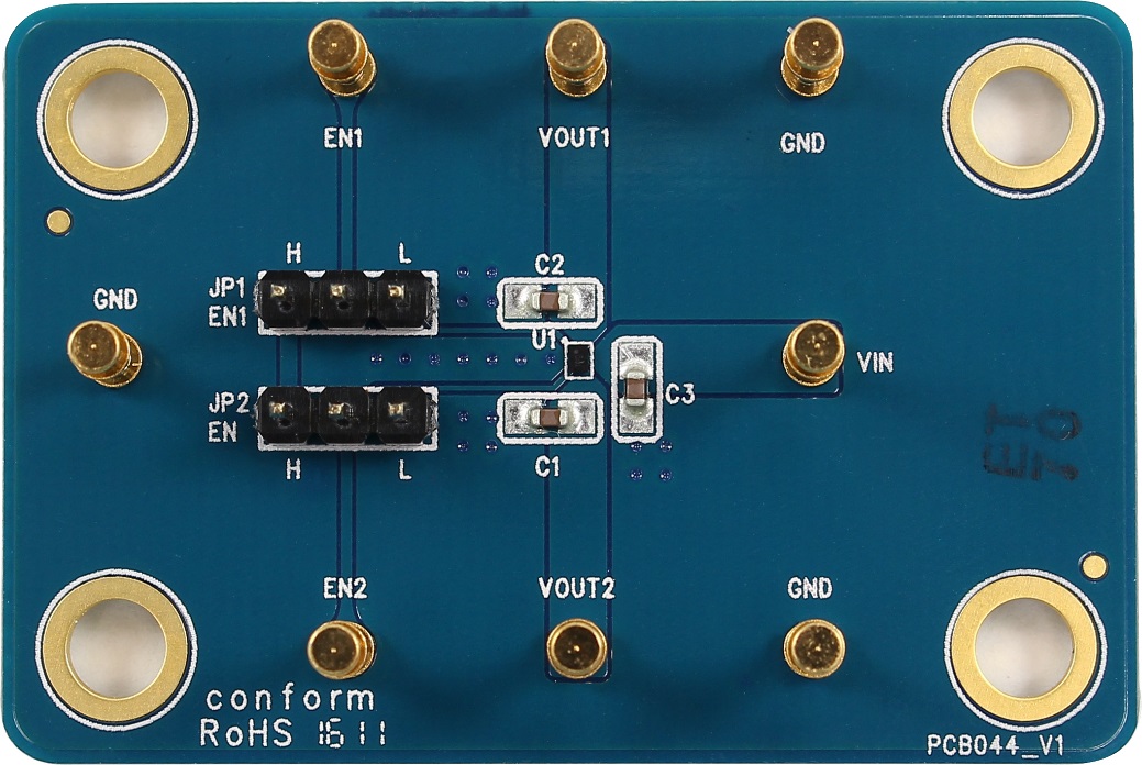
Please carefully inspect the EVB IC and external components, comparing them to the following Bill of Materials, to ensure that all components are installed and undamaged. If any components are missing or damaged during transportation, please contact the distributor or send e-mail to evb_service@richtek.com.
Test Points
The EVB is provided with the test points and pin names listed in the table below.
|
Test point/
Pin name
|
Signal
|
Comment (expected waveforms or voltage levels on test points)
|
|
EN1
|
Enable point
|
LDO1 Enable (Acitve High).
|
|
VOUT1
|
Output pin
|
LDO1 Output Voltage.
|
|
GND
|
Ground
|
Ground.
|
|
VIN
|
Input voltage
|
Power Supply Input.
|
|
EN2
|
Enable point
|
LDO2 Enable (Acitve High).
|
|
VOUT2
|
Output pin
|
LDO2 Output Voltage.
|
Power-up & Measurement Procedure
1. Connect input power (1.5V < VIN < 5.5V) and input ground to VIN and GND test pins respectively.
2. To use a jumper at “H” option to tie EN test pin for enabling the device. Inversely, to use a jumper at “L” option to tie EN test pin and ground GND for disabling the device.
3. Connect an external load up to 0.3A to the VOUT and GND terminals and verify the output voltage.
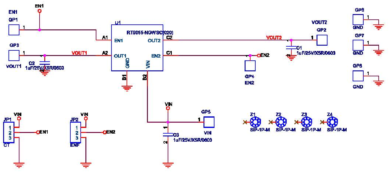
Schematic, Bill of Materials & Board Layout
EVB Schematic Diagram
Bill of Materials
|
Reference
|
Qty
|
Part Number
|
Description
|
Package
|
Manufacture
|
|
U1
|
1
|
RT9055-NGWSC
|
Linear Regulator
|
WL-CSP-6B 0.8x1.2
|
RICHTEK
|
|
C1, C2, C3
|
3
|
C0603X5R
|
1µF/25V
|
C-0603
|
TDK
|
|
JP1, JP2
|
2
|
|
Jumper
|
|
|
|
GP1, GP2, GP3, GP4, GP5, GP6, GP7, GP8
|
8
|
|
Golden Pin
|
|
|
|
Z1, Z2, Z3, Z4
|
4
|
|
SIP-1P-M
|
SIP-1P-M
|
|
PCB Layout
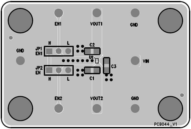
Top View
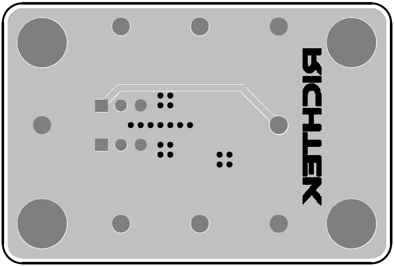
Bottom View